Digital Badge Design
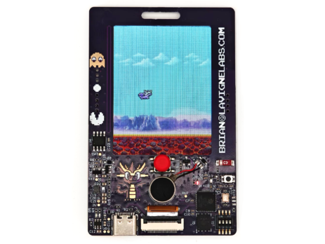
I’m going to Maker Faire in Shenzhen next week (November 16th, 2024) and wanted a digital badge. I was inspired by seeing other digital badges, but I wanted to add my own spin.
Design Goals
The badge needs to be eye catching, fun and low cost. I decided to base the design around an ESP32-S3 and a 2.4″ LCD.
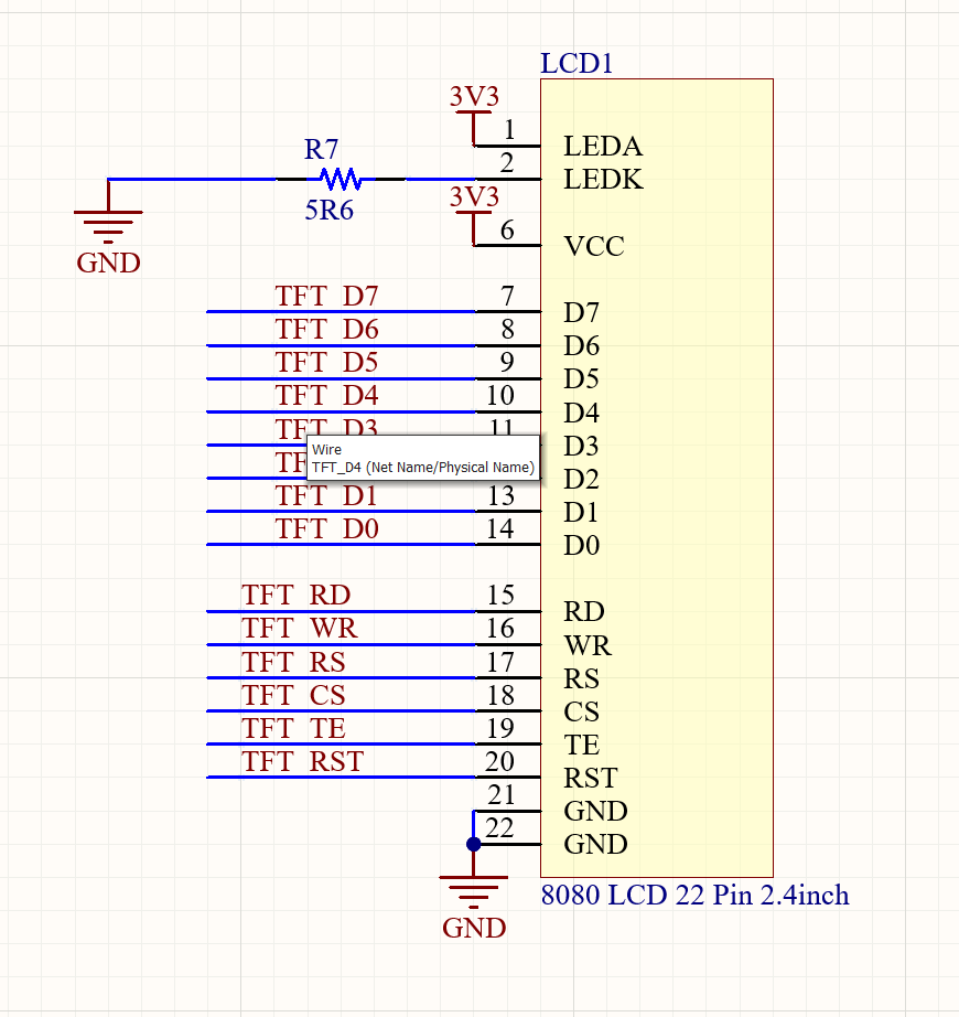
The first challenge as to figure out how to connect the LCD to the ESP32. I hadn’t used an 8080 interface before. In essence it’s 8 data bits and a 6 control lines giving a total of 14 GPIO. I decided to add sound and vibration to make it a bit more fun. Sound chip needs 1 GPIO, as does the vibration. I also need at least 1 button but decided to go with 4 DIP switches, a reset switch and the main button.
I wanted the main button to turn on/off the badge as well as be the input for the badge. I decided to make a Flappy Bird style game for the badge as the main display element. This is a great little programming challenge and provides a great progression for features to be added. I’ll get into the software progression later and it’s not finished yet!
Any ESP32 PCB layout can benefit from following the ESP32 hardware design guide.
LCD Considerations
The LCD is straight forward to connect. Connect each data line to a GPIO and we also have to drive the backlight. Often LCD backlights will need a boost controller but this LCD has all the LEDs in parallel with Vf of about 3V. There is the option to drive the backlight with a small constant current LED driver but seemed overkill for this badge. Instead, I chose to drive the backlight directly from the 3.3V supply and adjust current with a current limiting resistor. At 3.3V the resistor is consuming about 30mW which for this application is acceptable. I sized the 3.3V power supply to be able to handle the current draw of the LEDs + ESP32 + LCD + Motor all at the same time or about 300mA. I chose not to control the brightness, but this could be easily done with a PWM signal and switching element (P/N MOSFET or transistor). In a tradeshow setting I expect I will want max brightness at all times.
ESP32-S3
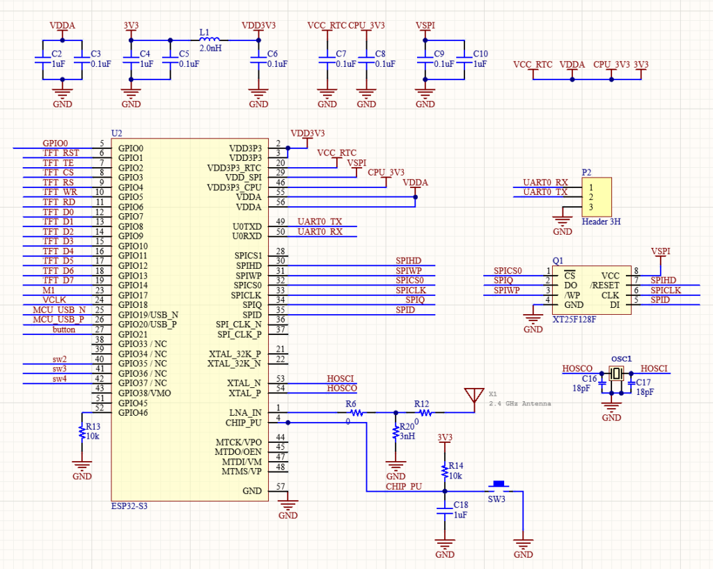
ESP32 has a number of power pins, each of which should have 1 or 2 capacitors placed in very close proximity, as well as 1 pin that needs to be pulled up on boot. The ESP32 needs both an external crystal and external SPI Flash. Some versions come with internal flash, but adding the footprint to the PCB for external flash makes the design more flexible. When laying out any MCU circuit it’s best to follow the assicuated hardware design guide very closely. The ESP32-S3 hardware desing guide has quite a few notes on how to limit interference for the radio. I wasn’t overly concerned as I don’t really need Bluetooth or wi-fi. That being said, I did go ahead and layout a the board with a small PCB antenna and tried to follow all recommendations. I haven’t analyzed the antenna yet, so I can’t say if it performs well or not.
Sound IC
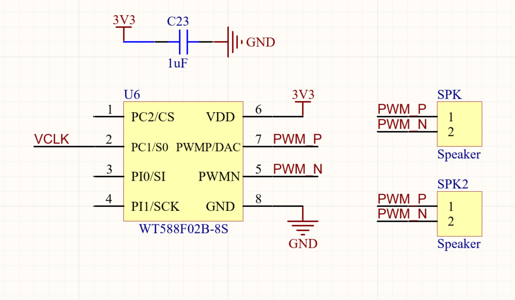
I used a Chinese programmable sound chip. You can load a bunch of sound effects on the chip and play each by sending a single command to the sound chip. This offloads all the work to the dedicated sound chip and requires very little programming. It’s also capable of driving a speaker up to 0.5W. I used 2*0.2W speakers to keep the badge as thin as possible. I re-used the sound effects from a previous project so it was very efficient to add sound to the badge.
Vibration
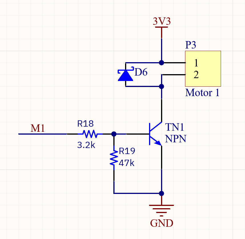
I decided to add a little haptic feedback motor to the design. There are several kinds, but the most suitable was a button cell battery style. These are completely enclosed and safe to touch when they are spinning. The downside to these motors is they actually draw a fair bit of current, so they can drain battery fairly quickly. There are several options to control them. You can add a small LDO to provide a lower voltage or PWM the signal to the motor. Since the motor I chose is 3.3V compatible, I chose to go the PWM route. I control the motor with a transistor and diode.
3.3V Power Supply
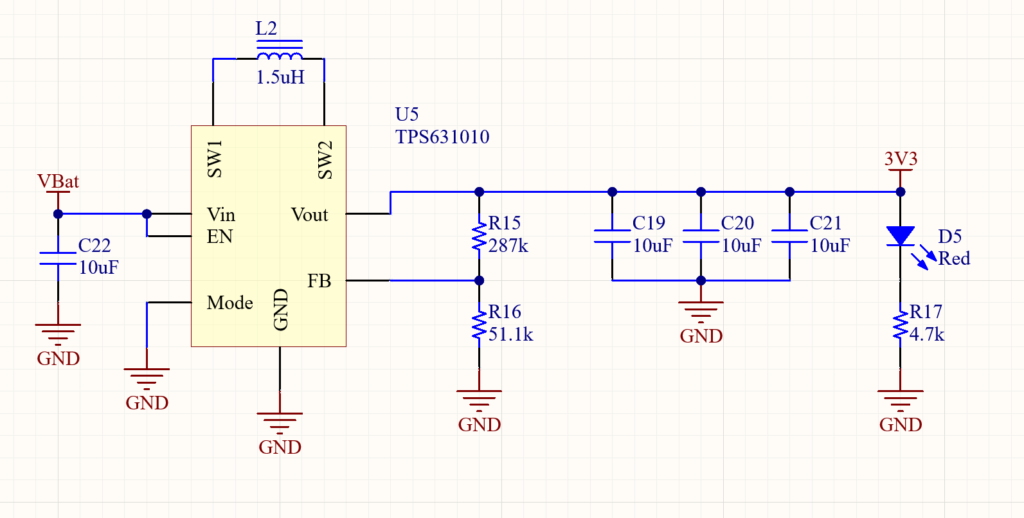
3.3V MCUs are a bit of a pain from a power point of view. We have these great lithium ion batteries that are cheap and powerful but they have a voltage range of 4.2-2.5V. What are we to do? We could use an LDO and simply accept we won’t be able to use the full battery capacity. This is really not a good option. If we had a 5V MCU it’s easy, we put a boost converter and we have 5V from any batttery voltage over the full range. Since we want 3.3V we could boost the voltage to 5V and then use another DCDC or LDO to convert to 3.3V. This works but efficiency isn’t great and/or we now have 2 noisy oscillators on the board. Considering we have a radio, and we care about battery life, this also not a great option. Don’t write it off entirely though, sometimes you need to use 2 switching regulators like that. That’s a discussion for another time. Enter the buck-boost converter. This type of converter can either reduce the voltage or boost the voltage and will give a stable output voltage from a range of input voltages below and above the output voltage. These are ideal but not plentiful, so selection is limited. I selected the TPS631010 from TI. It can deliver over 1A at up to 95% efficiency. There is better option for mass production but the MOQ made it unsuitable for this badge. This chip is mainly used in highly dense PCBs and is a small BGA package. The entire chip is about the size of a o402 resistor PCB footprint.
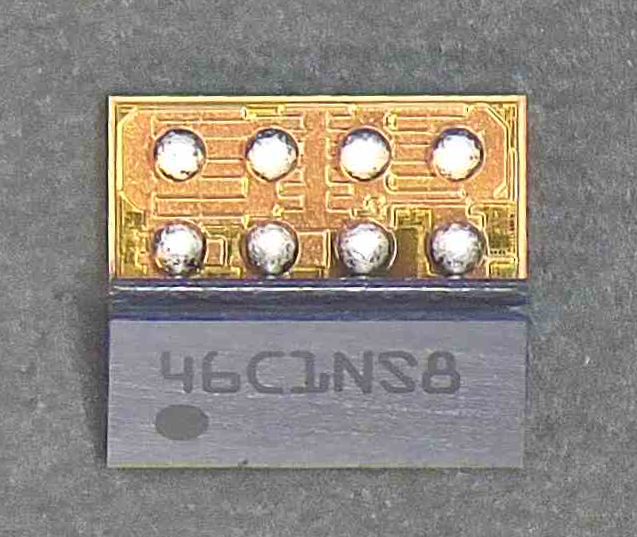
That’s a lot of pre-amble before we even look at the layout of the regulator but this highlights one aspect of design that can take a lot of time, parts selection. Suitability, cost, availability etc. all need to be considered. Layout for this regulator is straight forward and TI has great documentation.
Battery Charging
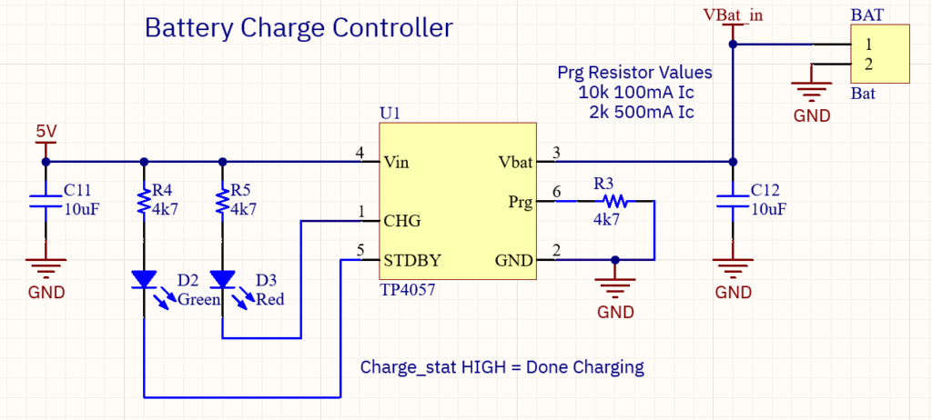
There are a lot of options for charging lithium ion batteries. To cut a long story short, the TP4057 is a good choice for this kind of project. Simple, cheap and plentiful. It can control 2 LEDs, for charging and charge complete indications and can directly power our circuit during testing while there is no battery connected. A single resistor sets the max charge current.
Push-on/Hold-off latching circuit
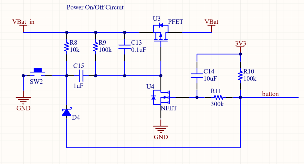
I took this circuit from mosaic-industries.com and modified it for purpose. It’s a latching circuit with 2 MOSFETs. The original design uses a single chip with 2 internal mosfets but I used 2 discrete mosfets. It’s very dependant on the Vf of the N Mosfet so it took a bit of tuning to get working. What makes this circuit attractive is that it’s instant on, short push, but takes 5s hold to turn off the circuit. This means re-using the button for input for our MCU is suitable as long as we only use short pushes. Less buttons are a good thing here. I won’t go into the functioning of the circuit but feel free to head over to the above link and check out the orginal post. I also changed the pull up resistor to 3.3V instead of Vbat so we don’t end up with 4.2V on an MCU GPIO, which would be bad.
USB C Port
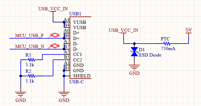
IMHO every design should only use USB Type C ports. There are a few things to pay attention to when using Type C ports. First you need to connect each CC pin to a 5.1k resistor so the connected hub knows to supply power. Next there are 2 sets of USB wires. This is a bit of a pain but once you solve the issue once, you can do it the same way each time. We will look at this in more detail in the PCB layout. Addionally we should add over current protection. I use a simple PTC for this purpose but there are other options as well. Similarly the data lines ideally have ESD protection, but since this is a development board, I’m omitting them. A consumer device should always have ESD protection on the data lines. I did add ESD protection on the VCC line, but this is likely overkill and can be left un-populated. For now, here is the USB Port schematic.
Next we will look at the PCB layout. Stay tuned!


