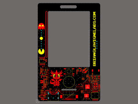
Digital Badge PCB Layout
I think this is the most fun part of every design. We’ve setup all the pieces for our puzzle and now we get to solve that puzzle.
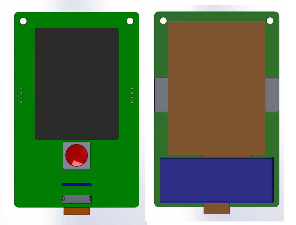
I did a quick 3D model of badge to find the location of the LCD cutout, ribbon cable slot as well as the size of battery I can fit. Once you have a 3D model of your PCB, you can import the outline to your PCB design software. I often make cutouts in my 3D so my imported outline also includes placement lines that I can use for my overlay.
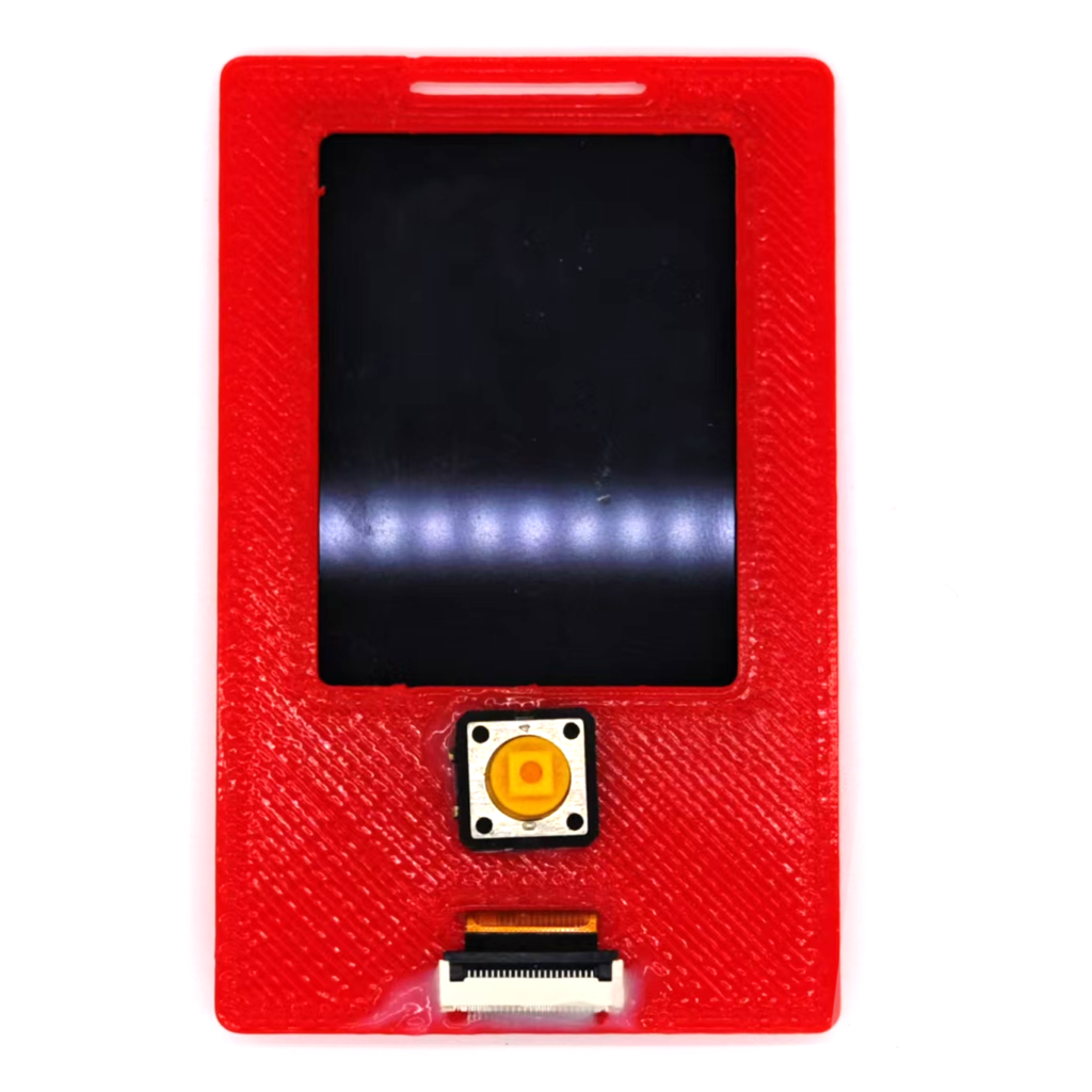
I 3D printed a quick test to make sure the connector and cutout were in the correct location.
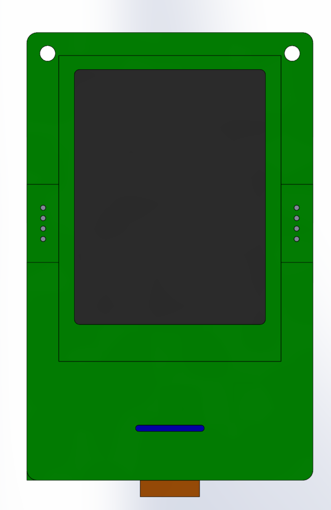
Here you can see lines for the LCD and speaker placements. I will place these on the bottom overlay layer in the PCB design so I know precisely where to stick the LCD. I also added a square corner for easily adding the origin.
Here is the final PCB layout and I’ll go over some of the areas you should pay attention to on a similar design.
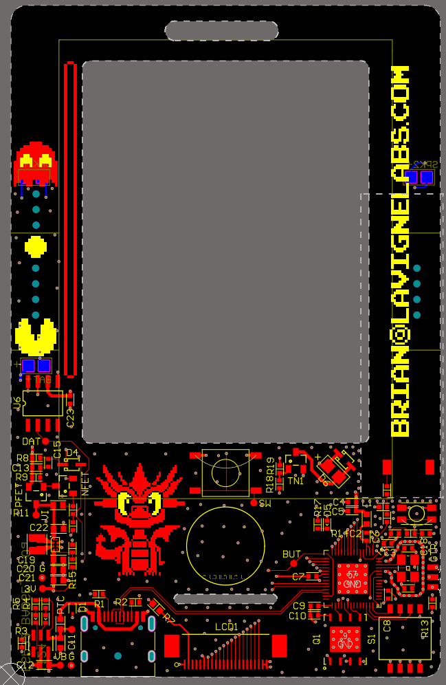
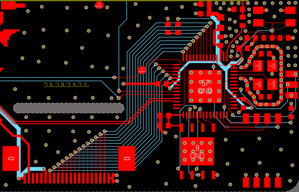
When laying out any PCB, I first place components that can’t be moved. In this case that is only the button and LCD connector. The next steps are an iterative process of laying out components to have the most efficient path. This is most important for critical data lines and high speed lines. Special attention should always be given to high-speed lines. Here we have the SPI Flash and USB port. USB Port can be placed anywhere and is only for debugging / charging so I don’t put much importance on its location. The Flash doesn’t have much option as to where to be placed relative to the ESP32, and neither does the crystal. I treated those 3 elements as a single chunk. Then I tried to orient that sub assembly to give the best path for the LCD data lines.
I should back up and discuss layer stackup. These days I design my personal projects mostly as 4 layer PCBs. It’s a bit more cost but it makes layout a lot easier. ESP32 guidelines suggest top layer for signals, layer 2 as GND, layer 3 for signals/Power/GND and bottom layer as GND. All signlas need a return path which is provided by the ground layer. Layers 1/2 are a pair and layers 3/4 are a pair. Layers 2/3 are physically very far apart, so typically would not be considered a pair.
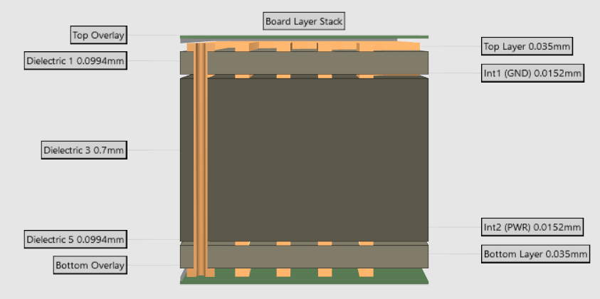
For a real world example, this is a 1mm JLC PCB 3313 4 layer stack up. The situation is even more extreme on 1.6mm PCBs. The closer layers are together, the better the return path and the closer the coupling. In fact high speed layout is not my expertise so I’ll limit my comments on this subject. I can refer you to experts like Eric Bogatin, or videos with Robert Feranec.
Let’s examine some details in my PCB layout. We have the ESP32 and SPI Flash connected with very short connection and a I used a standard layout for the crystal. There is a good general application note on laying out crystals for STM32 MCUs but the principles are common to all crystal layouts. In general, it’s hard to layout a crystal so poorly it won’t even function and there is quite a bit of wiggle room in the “OK” range. I’ve never achieved “Perfect” so don’t take my layout at the best.
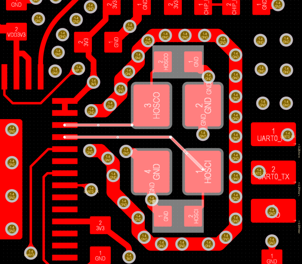
Keep lines short and don’t run anything under the crystal. You can put a guard ring around the crystal to help with EMI. It’s also ideal if osc lines are equal length, and don’t place the crystal too close the PCB edge if you can help it. I’ve never been able to follow every rule in a single design, so do your best and it will almost certainly work.
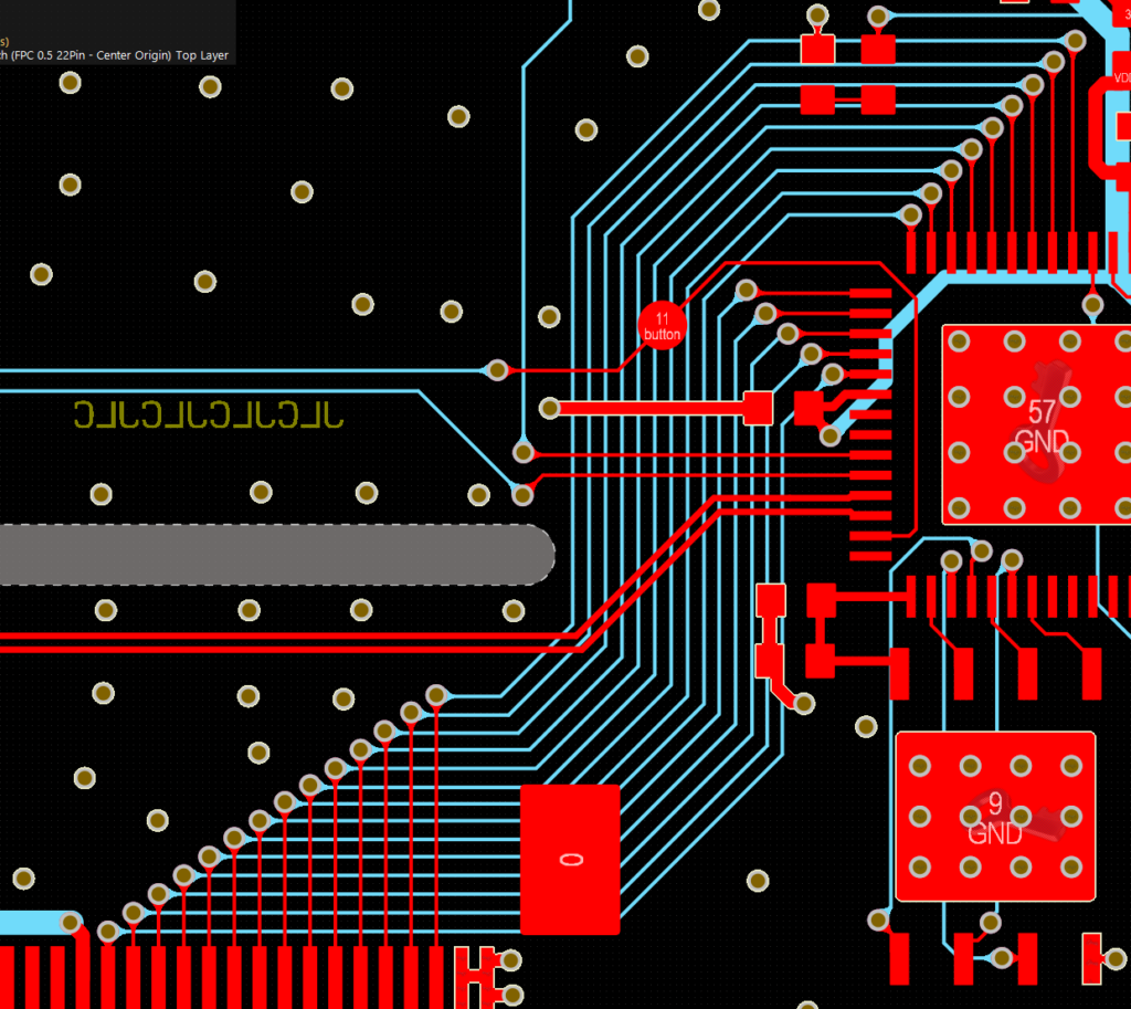
PCB layout is a funny thing. You might see my layout and think that was clever or you might immediately see that by reversing the GPIO order, I could have saved crossing all the data lines. I’m not unhappy with the routing and it ensures the USB lines stay on the top layer. I’d have to try the alternate layout to know if it really would be better. It’s perhaps a good example to show there is not just 1 way to work things out. There might only be 1 “best” way, but a whole lot of solutions that are “OK”. There are a lot of subtleties in laying out PCBs, especially with high speed signals.
There are some considerations to laying out the antenna, but I’ll leave it very general as I have not classified the performance yet. I used a chip antenna which is very dependant on GND copper area and location on the PCB. Follow manufacturer guidelines. Use rounded paths for all feed lines as sharp angles can cause signal reflections (power loss).
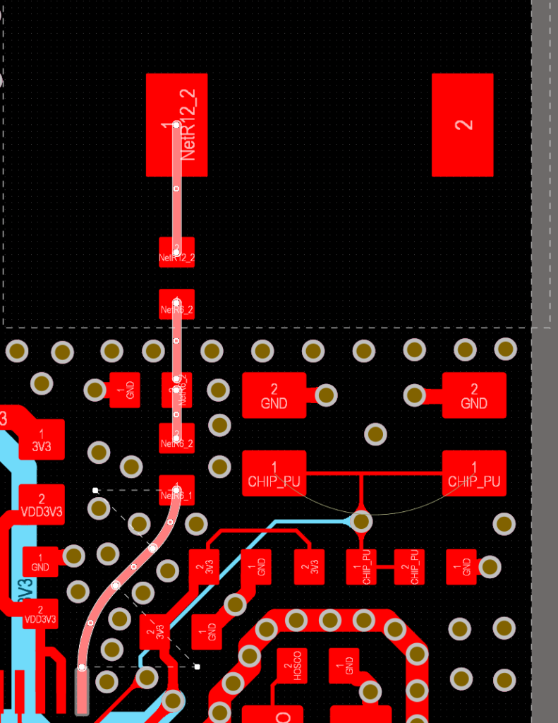
Respect datasheet layout requirements for distance from PCB edge, feedline impedance, tuning network and GND layer area. These antennas are very dependant on GND layer area. This is now way beyond what I’m comfortable giving advice on, so let’s move on.
The Buck-Boost converter always needs a bit of consideration. Keep it physically far from sensitive components (antennas) and keep your current loops small. Manufacturers usually have a pretty good layout example in the datasheet.
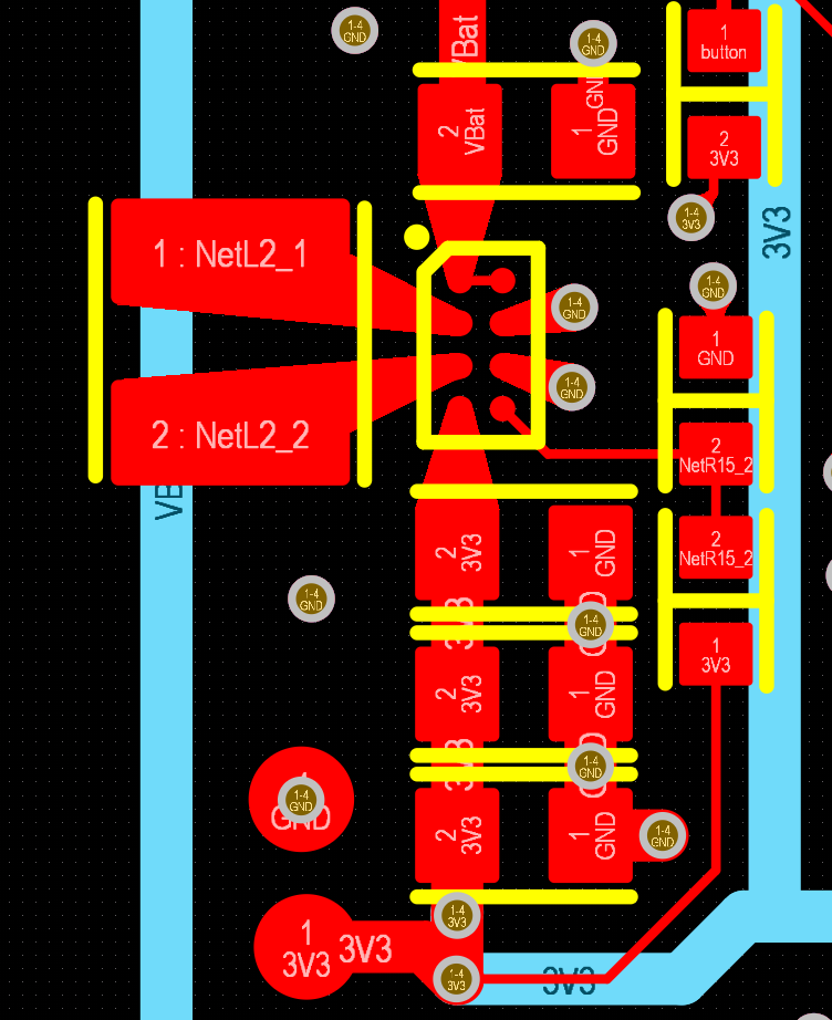
Inductor, input and output capacitors close to the IC. Widen traces as much as needed for current and heat syncing but don’t go crazy with copper on the inductor. There is a feedback line for voltage regulation. Your feedback should be connected after all the output capacitors. similary connect your output voltage to the power plane after all the filter caps. Quality of output caps is very important, but space constraints directly conflict with this. Do your best. I’m using X5R 0603 caps, but of course X7R 1206 would be much better. x5R/X7R refer to the change in capacitance with temperature. X7R are generally rcommended for converters. The datasheet says X5R will work. Experts in layout will find places my layout can be improved, but this one is generally OK. Don’t be scared to layout switching converters. There is a lot of room in the “OK” range. “Perfect” is always hard. There are many factors that affect “perfect” and even for experts, there is an initial layout, physical testing and tuning. If you don’t have radios, sensitive high speed lines or need to pass EMI testing, literally any layout will function. That’s not to say you shouldn’t follow guidelines, only that you shouldn’t be afraid to layout a converter. They are essential in todays PCB designs. This topic is a very deep rabbit hole. The switching mode of the converter, switching frequency, load etc. all factor in to EMI. Let’s leave it here for now.
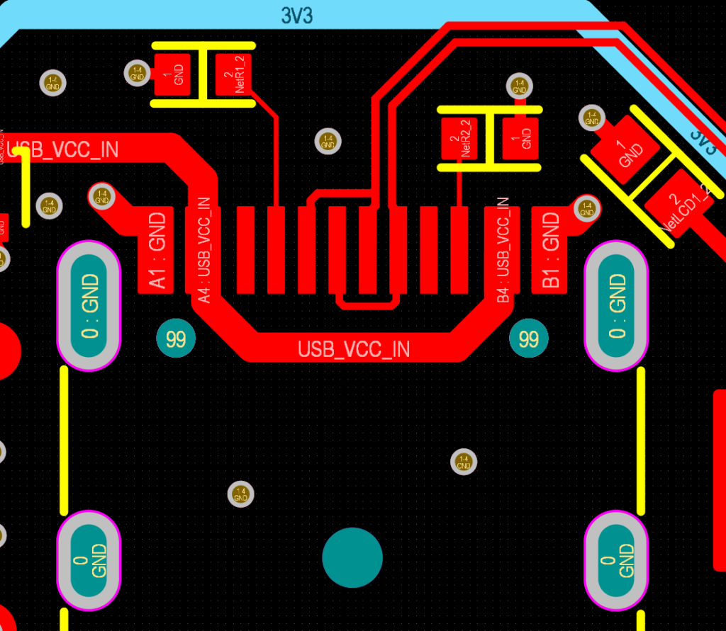
Here is how I layout USB Type C connectors. Remember I left off the ESD protection on the datalines, but otherwise this is an OK layout. Why are USB Type C connectors a bit of a pain? I’m talking about USB 2.0 layout, let’s leave USB3.1 for another day. They are a pain because they are double sided. We don’t know which pair of wires will be used so we have to wire both. You could just wire one pair, but then you have a 50% chance you need to flip the connector to have it function. This isn’t always a deal breaker, but let’s wire up both sides.
Power is easy, just connect both power pins with a thick trace. Similarly ground both sides of the connector. We need to have a seperate resistor for each CC line but they don’t need to be close to the connector or anything special. The differential pairs are a bit more complicated. I have found no perfect way to connect them. There is always a trade off. The good news is that as long as you don’t have very long lines, it basically always works. Layout diff pair with the proper impedance as per your software or PCB manufacturer calculator. If the lines are short enough that’s not even needed, but best practice is use proper impedance. The complication is how to wire up 2 pairs. There is always going to be a split, or via with something crossing to the other side of the PCB. This creates a length missmatch. The way I laid it out on this PCB is not uncommon and should work for most situations. This is far from the only solution I won’t claim it’s the best. It is however convenient.
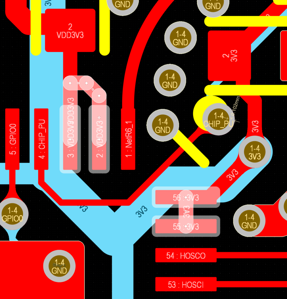
A general comment about pins that are wired together. I try and always connect pins together like pins 2 & 3 in the photo. Due to space limitations I connected 55 & 56 with a jumper but this was only due to space.
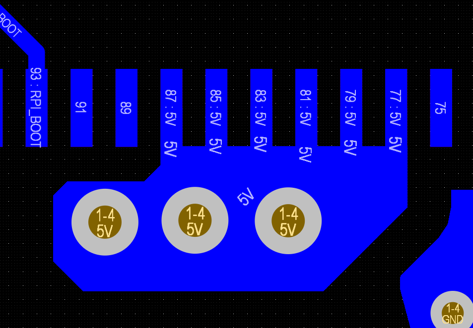
This is from a different PCB, but it’s a more extreme case. I find less production issues with this method. Call it personal preference if you like, but I do prefer it.
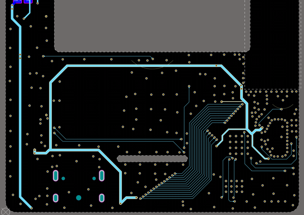
Let’s take a quick look at layer 3. I’ve laid out the power rails as traces to visualize the paths. Make sure that my signals don’t affect them. Then I apply polygon pours over these areas for best performance. If needed you can remove the traces after. The main reason to remove them would be to allow for GND via placement in those exact locations. Since there is a pour, there is no reason that exact spot can’t have a GND via, but it was not an issue, so I diidn’t remove them.
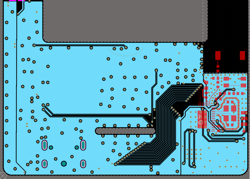
This is the same region after the pour is applied. I overlaid part of the top layer to show there is full GND under both the crystal and the antenna feed line. This is recommended in the ESP32 design guide. Under those locations are 3 complete layers of GND pour L2/L3/BL.
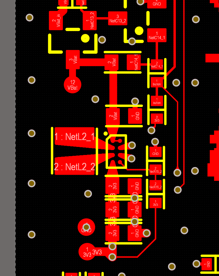
It’s a good idea to add test points to your PCB. These serve a number of purposes. First, as the name implies, they give you a convenient location to measure signlas. They also give you locations where you can hack signals, cut traces and solder wires. In development it’s not always possible to be perfect on the first attempt and this can make an otherwise flawed board completely functional for testing. Soldering directly to pins etc is possible but this is much easier. With signals, it’s not important how thick the connection between the test point and the signal is. We will only ever connect a multi-meter or oscilloscope. With power test points though, I try and make them thick enough to support the full load current. That way I can directly test a converter/battery charger/soft latch etc. with an electronic load at full current and have a nice place to solder my test leads. You can always solder directly to capacitors and the like, but this is much less likely to damage your board. They are also good practice for when you do production PCBs that need to use automated testing equipment that uses pogo pins.
Wow that was a lot to say about a tiny PCB made just for fun!


