PCB Artwork
Have you ever wanted to add some images to your PCB designs? I think of PCB artwork as similar to easter eggs in video games. Very few people will ever see them, but just knowing they are there is nice. No matter if you think of them as showing off, a signature, easter egg or just part of the design, I’ve got some tips that might help.
PCB Structure
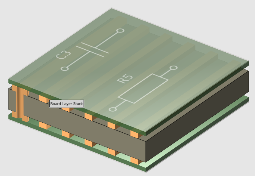
Let’s discuss very briefly how they are made. The raw PCB material is copper clad board, often made of fiberglass. This copper is etched to form the traces of the PCB. The traces are “masked” so they are not removed during the etching process. This is called “Top Layer”. Next the PCB is covered with an insulating layer called “Resist”. This is some kind of polymer, epoxy or similar coating. It must be heat resistant and isnlulating. To solder to the copper traces we need holes in resist layer. This is called “Top Solder” and represents areas that do not have resist. Since bare copper oxidizes rather quickly, the exposed copper is typically covered in either solder or gold. Last by not least, lettering is printed on the PCB called “Top Silk”. Typically, lettering never overlaps any areas in “Top Solder”. If there is overlap, the manfucturer simply doesn not print the overlapped areas. PCBs often have multiple copper layers and connections between the layers called vias. We will use Top Layer (copper), Top Solder(no resist) and Top Silk (printing) for our artwork.
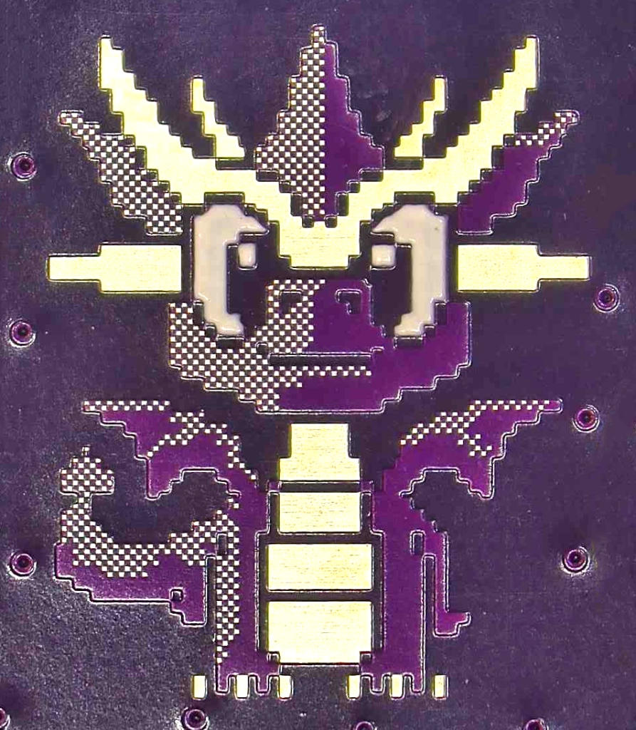
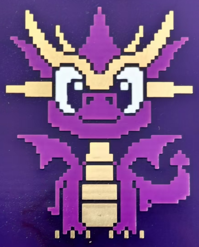
The most obvious PCB artwork is simply an image on the Silk Layer on your PCB. This gives you a 2 color image and adds something for sure, but we can often do better. If you can’t use copper in your design, you can still add some kind of dithering to your image to simulate a 3rd color (PCB is the first color with Overlay being the second). In the dragon logo on the left you can see dithering was used on the left side of the face, top of the wings and tail. Each square is 0.1mm and when zoomed out, gives the illusion of light purple.
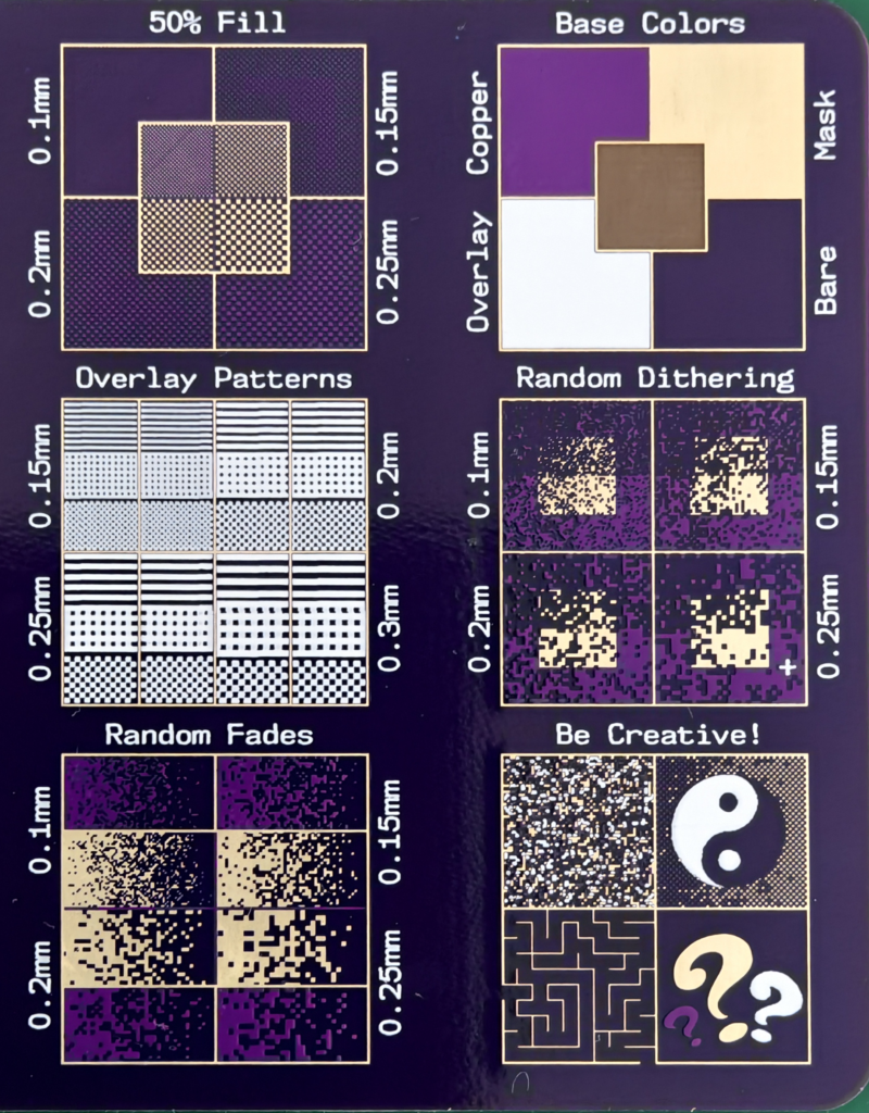
Here are some examples of dithering with the Overlay. There are 3 types of dithering patterns shown at various sizes. We have lines, grid and checkerboard patterns. You can also try random dot patterns or something more creative. If you do go for random dots, I would suggest 0.2mm or larger to make sure they fully print. This is completely dependent on the manufacturer and the printing type.
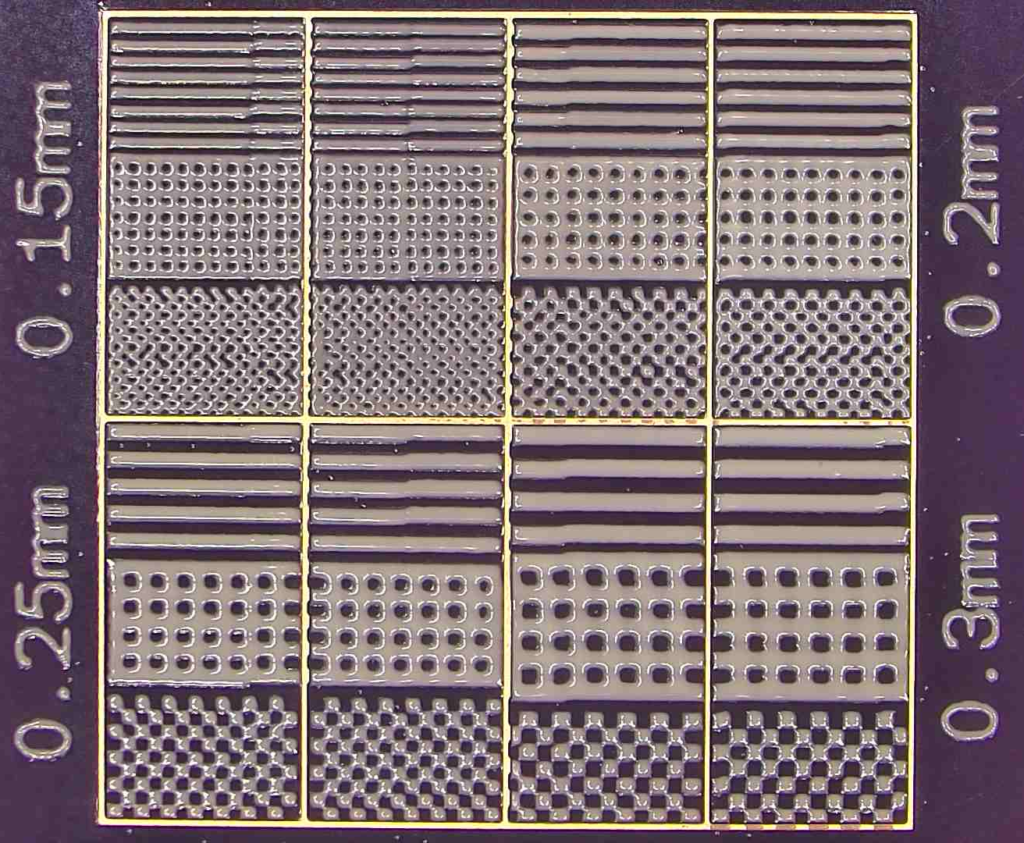
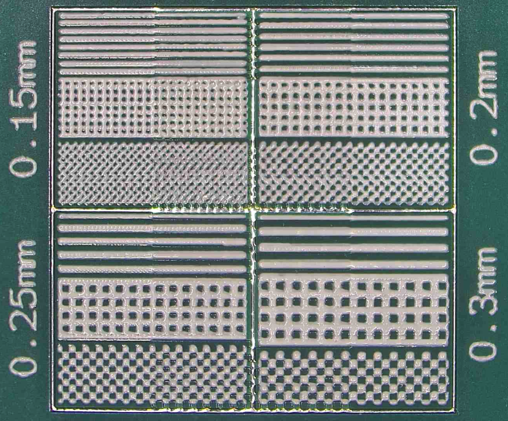
If you can use copper for your design, you open up a lot of options. First we now have 5 base colors: Dark Green, Light Green, Yellow, Silver/Gold and White. These correspond to various layer combinations, and I use green as an example, but it could be purple or whatever color you use for your PCB. Quick Note, black PCBs typically have no differentiation between Light and Dark, so I’d say they really only have 4 colors. Also if you want to get really creative, with gold PCBs, you can add paste mask to some areas to include silver and texture in your designs, but I digress. Let’s look at the standard base colors.
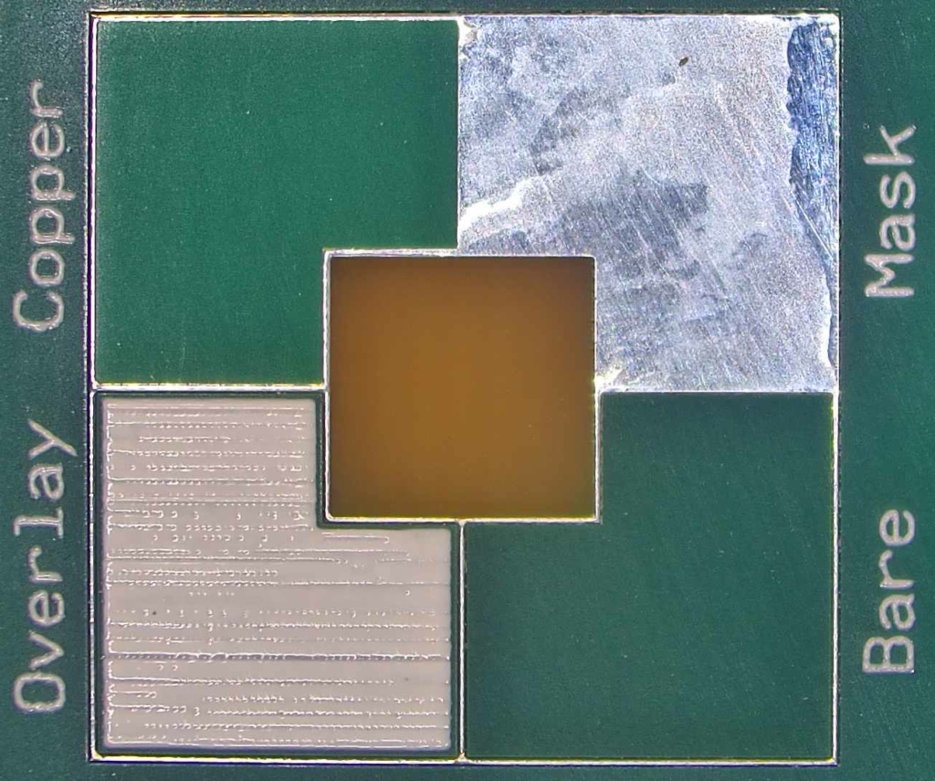
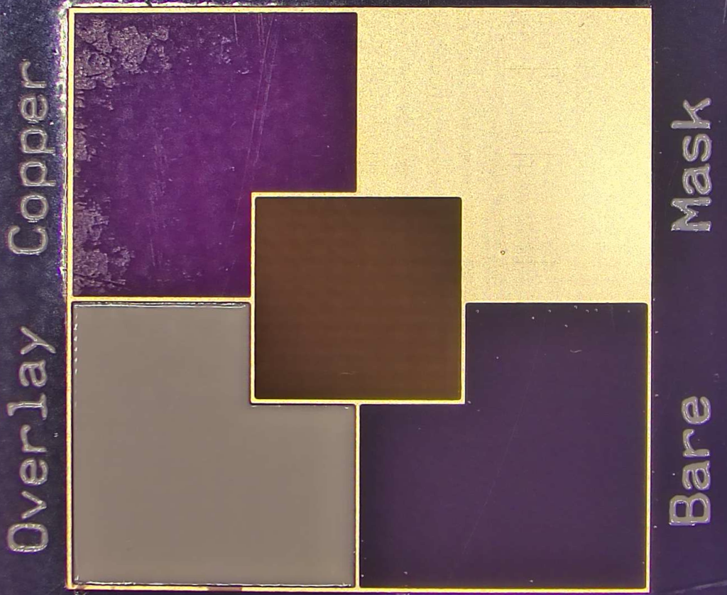
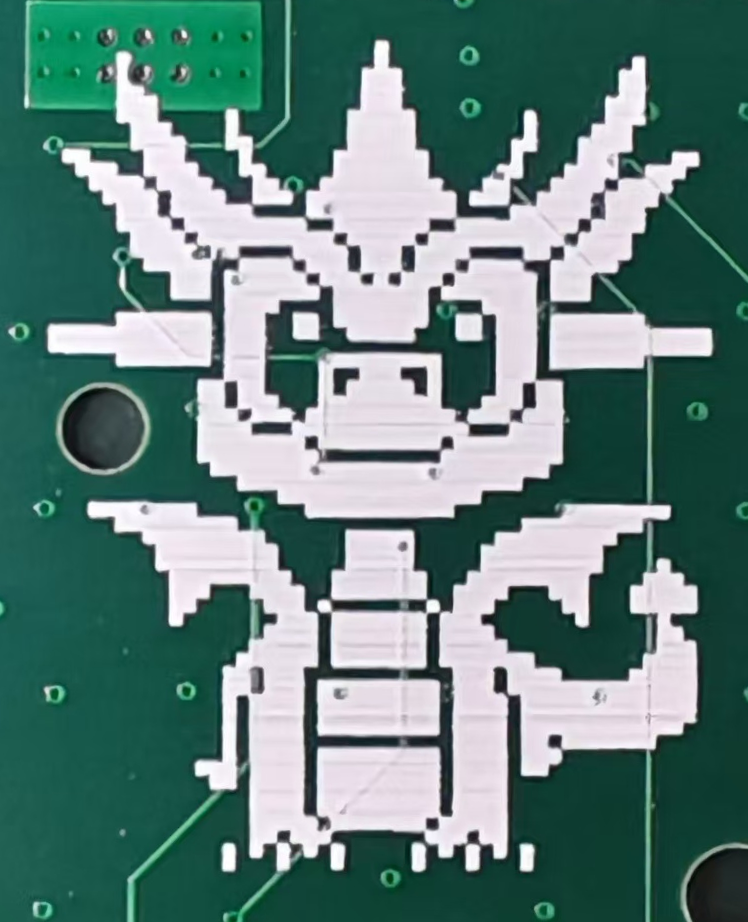
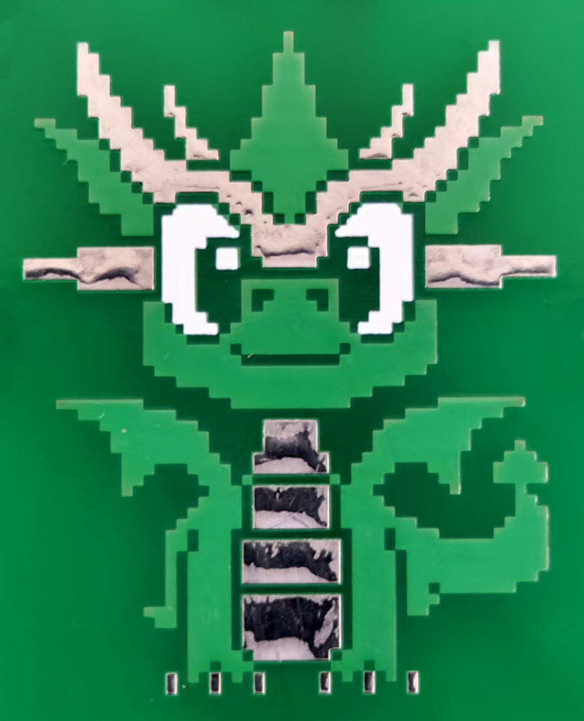
Starting at the top left we have Top Layer. TThis we will call Light Green. The Bottom right is empty on all layers. The center is Solder Layer with nothing else on any layer. The top right is effectively a solder pad, which might be silver, gold or even copper depending on your production options. This is Top Layer + Solder Layer. The bottom left of the image is the overlay layer. Notice the purple PCB has high resoution printing and the green PCB has standard printing. Overlay can print over Top Layer, but not the mask layer. Typically overlay is pulled back, maybe 0.1mm, from pads and must be minimum line thickness of 0.1 or 0.15mm to be printed. In my experience 0.15mm*0.15mm dots usually show up to some degree. If you look closely the overly on the purple PCB is much closer to the gold tracks than on the green PCB. On this PCB I requested no pull-back on the overlay layer. It makes things much more sharp. Here is another example to show the difference.
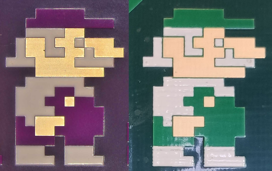
Now that we have the basics out of the way, let’s talk about the fun stuff. The copper layer. PCB manufacturers are extremely good at etching copper. Very fine details can be achieved. It might be counter intuitive as the Overlay Layer is used for marking but the Top Layer + Overlay Layer gives the highest resolution, highest contrast results.
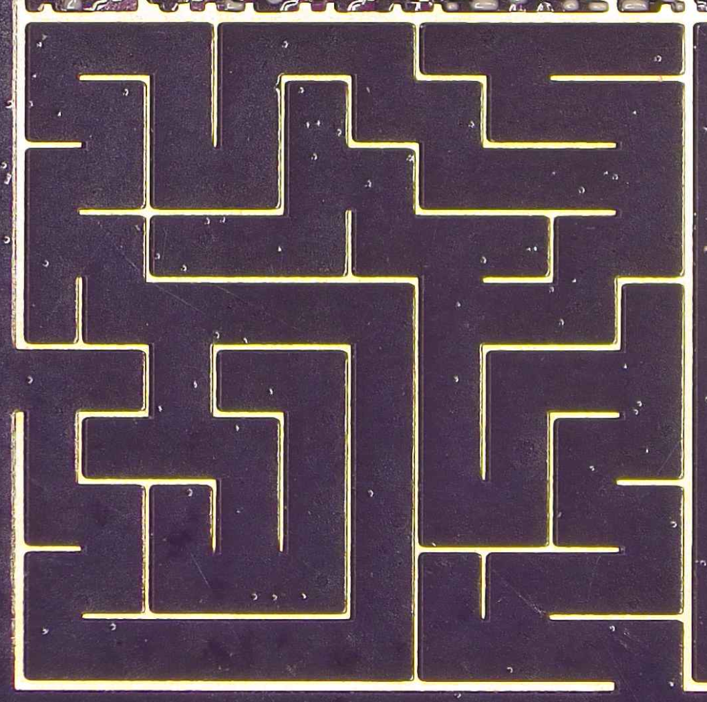
This is a 0.1mm line on the copper and mask layers. The maze is 7.5mm square. You can see the detail is very fine. Not surprising as this a standard track size available for standard manufacturing. We can apply this to our logos and artwork to great effect.
Let’s look at some dithering patterns:
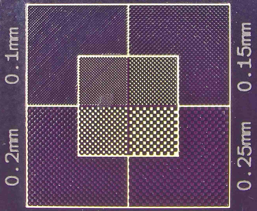
Here we have checkerboard pattern fill. There are 2 layers where this is very effective, Top Layer & Mask Layer. From a distance this gives either a lighter PCB color or darker PCB color depending on which layer you choose. In the headline picture of this post you can see a dragon with 50% checkerboard on the mask layer over Top Layer that gives a great light purple effect (PCB color is purple). Anything smaller than 0.1mm squares are likely to not turn out. PCB manufactures take our submitted designs and modify them for the actual manufacturing process. They need to expand the copper regions to account for the effects of etching. I’ve overlaid the expanded copper drawing on top of the actual PCB. This also means that small squares are really round hole in the copper like below (0.1mm checkerboard).
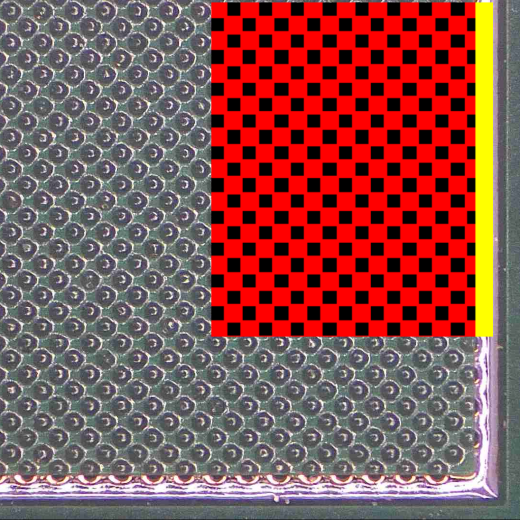
I have also produced a board with no expansion of the copper. This produces a nice but different effect. You cannot do this if you PCB is not purely art. It will certainly affect actual pad sizes. I expect that the expansion is about the same thickness of the copper layer.
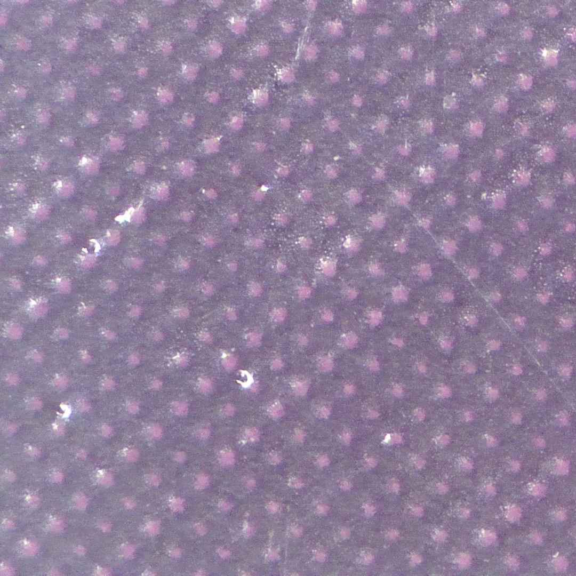
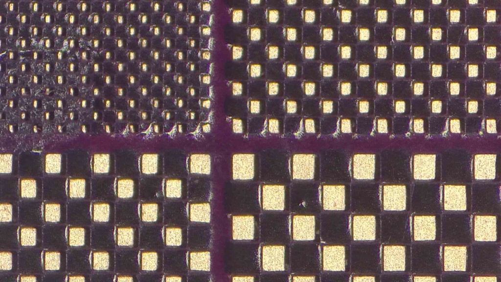
You can see how the squares on the 0.1mm size don’t connect and appear as small dots, where as with expansion we end up with a grid of holes.
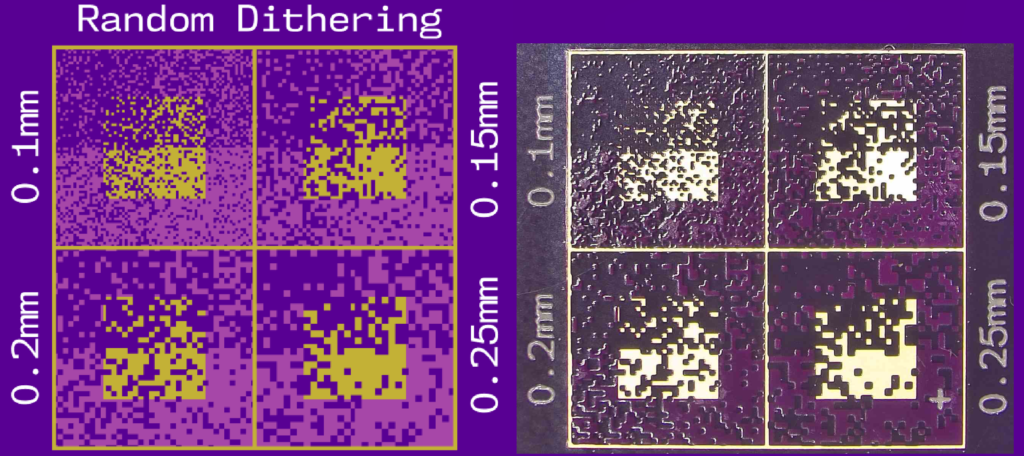
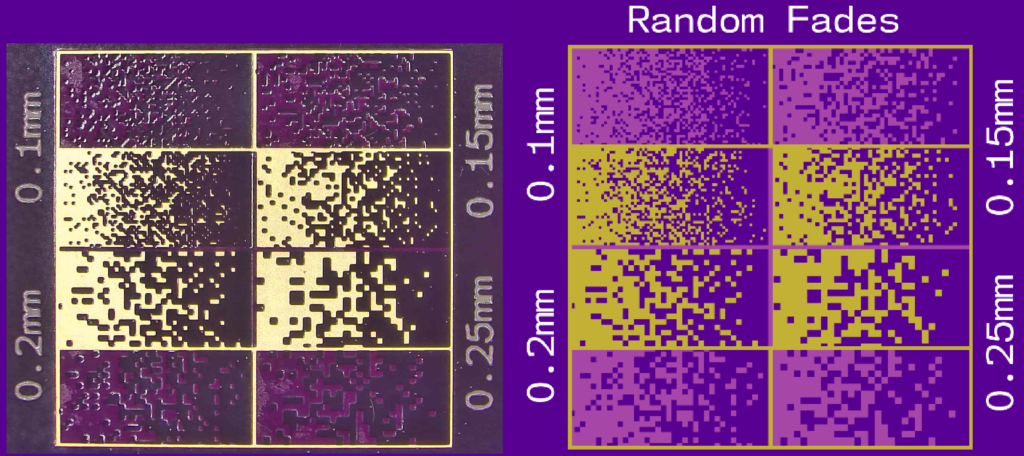
Here are a few other dithering patterns I’ve tried. I’m sure there are many more I haven’t thought of that you can try.
Laying out the graphics
The first layer I place on the PCB is the copper layer. Copper layer is base layer of the image. Let’s build up Shiverwing to see the steps.



First we add a copper layer which includes solder layer and usually overlay as well. I find overlay on top of copper looks a little bit better. Next we add the solder layer on the parts we want to be silver/gold. Finally we add the overlay for the white highlights.
Lining up graphics
Laying out the graphics on the PCB depends on what software you are using. In Altium this is a good procedure, so I’ve heard. I don’t use Altium myself:
- Create your graphics so all the images are the same size. I use different layers in Photoshop and export each one separately as a black and white PNG8. Remember Images should be black and white only, with black being the image and white the background. Image should be high resolution, 125dpi works very well.
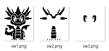
2. In Altium create a rectangle representing the image size you want on your PCB. I place this on a mechanical layer.
3. Enable snap to for all layers
4. Activate the destination layer, say Top Layer
5. Place graphic and select the rectangle
6. Import your image at 125dpi.
7. Repeat for all layers
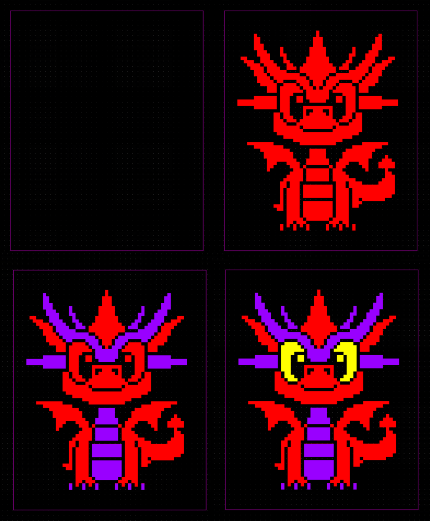
Optionally you can create union from all objects. Now you have a graphic in your PCB you can move around.
KiCad Layout Procedure
Coming soon. Stay tuned!
PCB Art Gallery
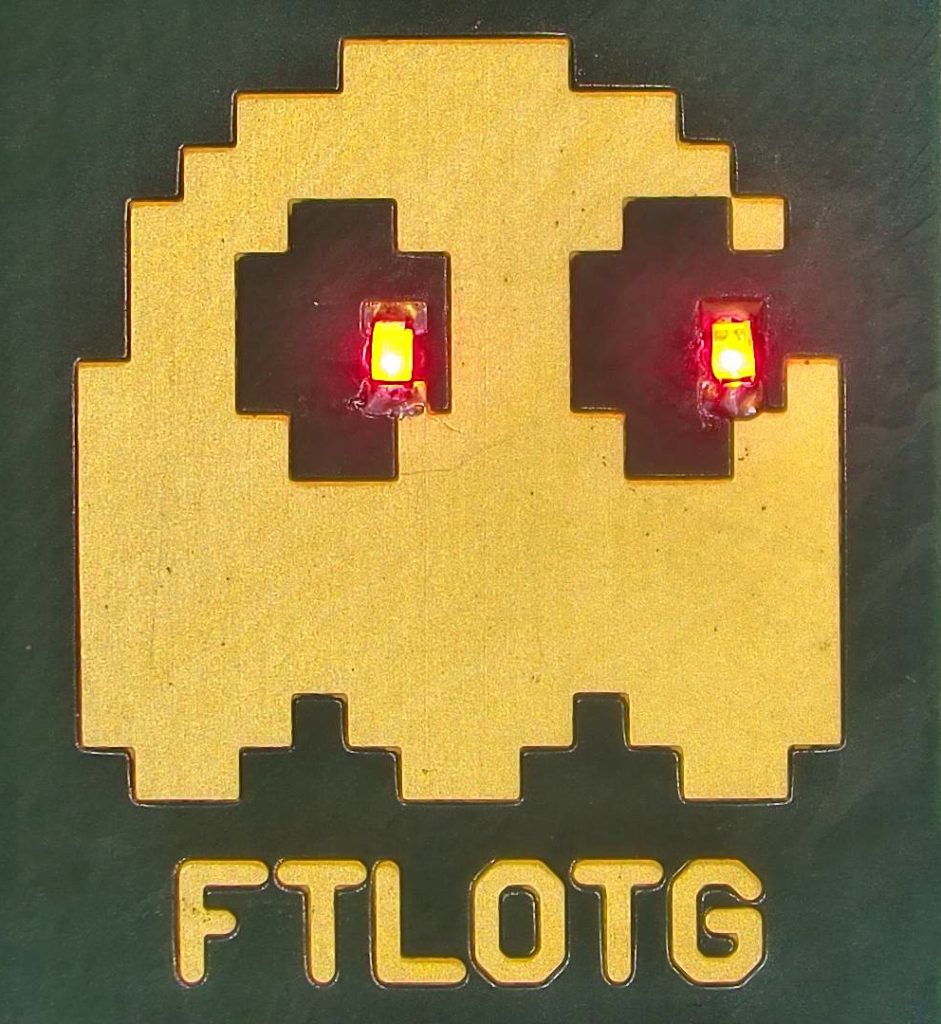
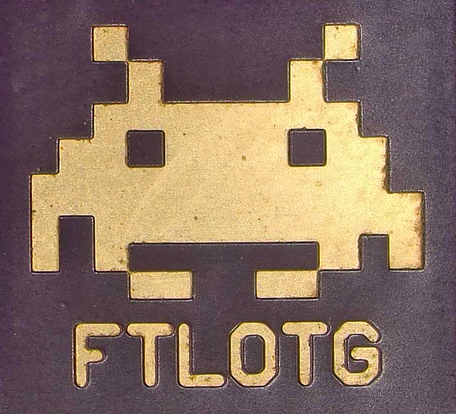
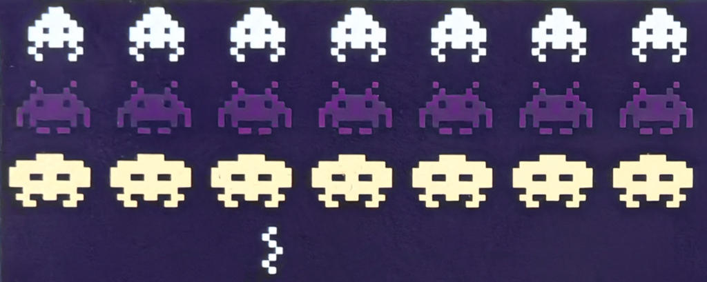
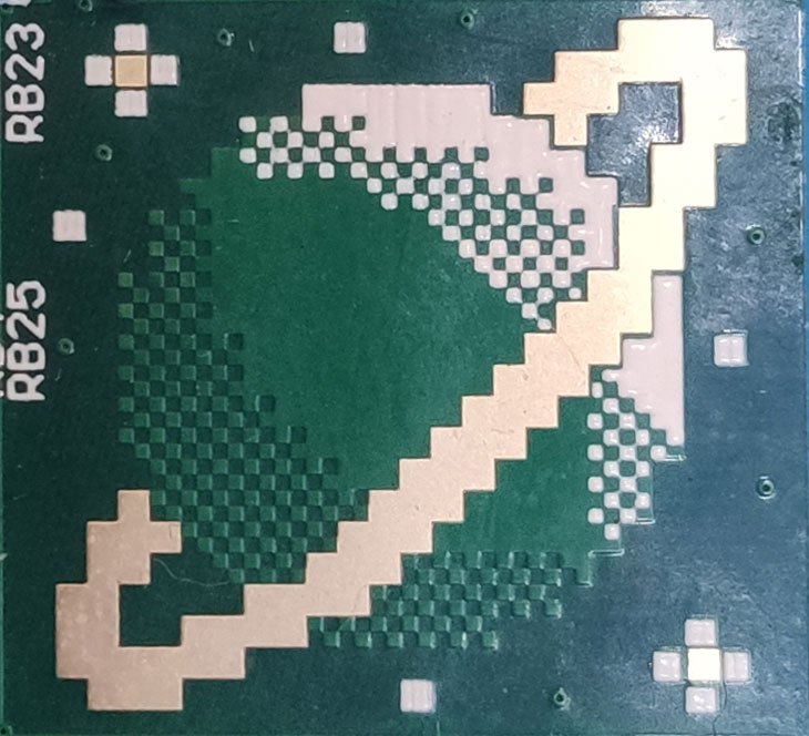
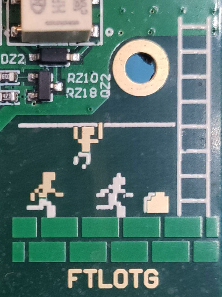
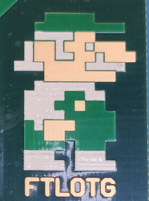
Here is a gallery of some pixel art I converted to PCB
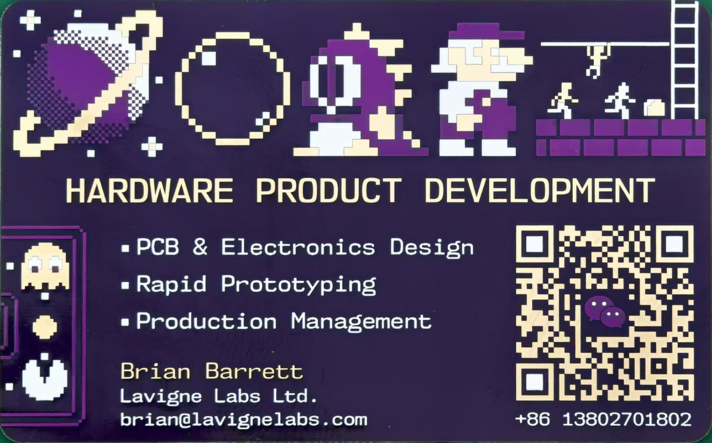



Don’t forget to have fun!


